03 — Hardware & Electronics
Built at the physical layer
The boards, the silicon, and the bench they are made on.
PCB development, SMD and SMT microassembly, and biomedical microchips — designed, milled, soldered, and enclosed on equipment I own, then integrated into the devices and machines that use them.
My hardware work runs from the schematic down to the bare die, and back up to the finished device it lives inside.
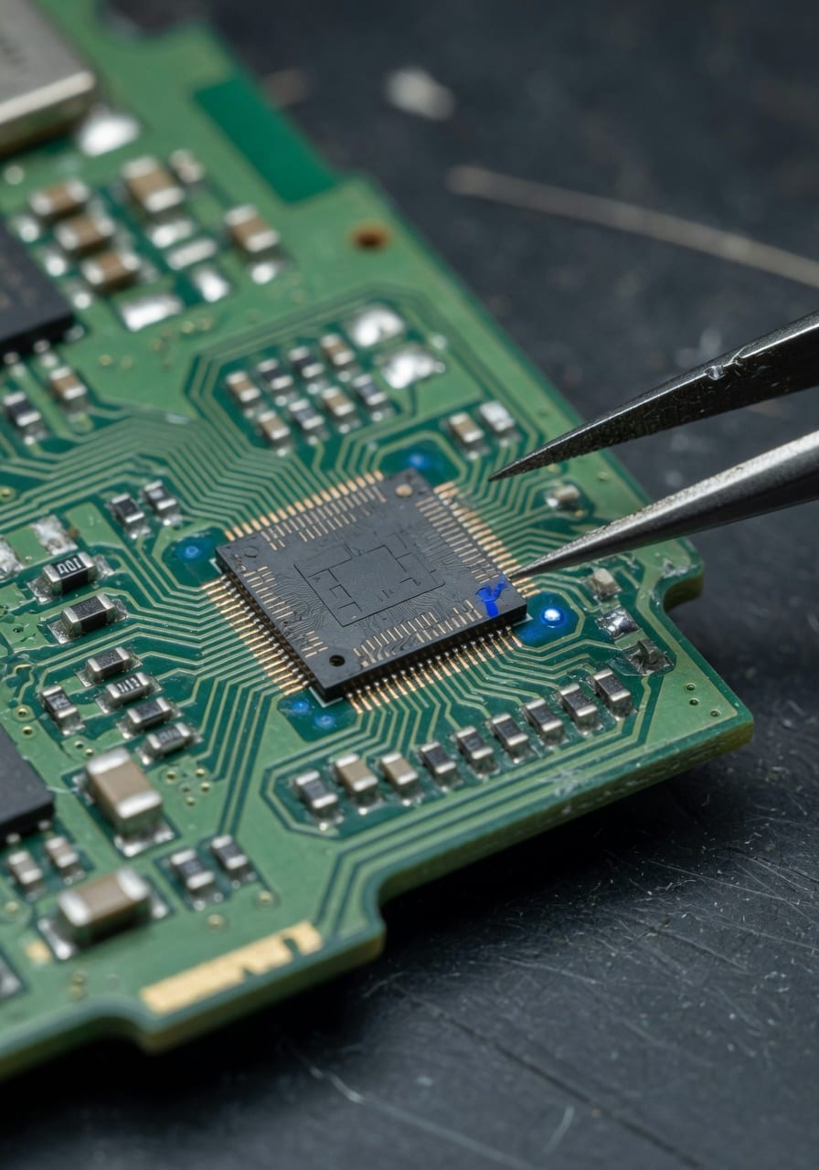
I develop PCBs and do the microassembly myself: SMD and SMT placement of fine-pitch parts, and the microsoldering that goes with it. The scale of the work has moved from board-level electronics into microelectronics and nanoelectronics — components small enough that the microscope is not optional but the primary instrument on the bench.
The bench is mine end to end. Microscopy and microsoldering equipment for the small work, a CNC machine for in-house PCB production, and an FDM 3D printer for the plastic enclosures, covers, cases, bases, and mounts that house each device. That ownership is what lets a design move from layout to a tested, housed board without an external fabricator in the loop on every revision.
From there the work is integration. Embedded SoC integration puts the silicon into a finished product; robotic systems integration puts a microchip control plane in command of the mechanics. The chip senses, decides, and drives — and making that reliable inside a larger system is the part that takes the breadth.
edge length of the complete vitals module — a full subsystem inside roughly 1.5 × 1.5 cm
footprint class of the nanocomputers I design around at the die level
vital signals fused on-module: heart rate, temperature, and SpO₂
of the bench is mine — microscopy, microsoldering, CNC PCB milling, and FDM enclosures, in-house
A complete vitals system the size of a fingernail.
The biomedical microchip
Roughly 1.5 × 1.5 cm, with everything a wearable needs already on board.
I design biomedical microchips around MEMS sensors that monitor heart rate, temperature, and SpO₂ — blood-oxygen saturation. The target is not a sensor breakout but a complete system in a footprint around 1.5 × 1.5 cm.
Inside that area sits its own microcomputer, the MEMS sensors, a signal concentrator that gathers their outputs, an algorithm processor that turns raw signal into vitals, a Bluetooth antenna for the link out, micro LiPo batteries, and wireless charging. The whole acquisition-to-transmission chain is on one small board.
- MEMS sensing for HR, temperature, and SpO₂
- On-module microcomputer and dedicated algorithm processor
- Bluetooth out, micro LiPo power, wireless charging in
The signal path, drawn out.
MEMS module — block diagram
Sensing, concentration, processing, and link — on one substrate.
The module is a small pipeline. The MEMS sensors feed a signal concentrator; the concentrator hands a clean, aggregated stream to the algorithm processor; the processor produces vitals that the microcomputer transmits over the Bluetooth antenna. Power and wireless charging sit underneath the whole chain.
Drawing it as a block diagram is how the placement gets decided: the analog front-ends stay close to the sensors, the RF section stays clear of the noisy supplies, and the charging coil gets its own zone.
A revision, start to finish.
One board, one day, on my own bench
- 01 Design Schematic capture and layout for the board, the sensor placement, and the RF section.
- 02 Mill CNC routing of the PCB substrate in-house, no fab lead time for early revisions.
- 03 Microassembly SMD and SMT placement of passives, the SoC, and the sensor package under the microscope.
- 04 Microsolder Reflow and hand microsoldering of fine-pitch parts with the magnified bench setup.
- 05 Enclose FDM-printed plastic case, cover, base, or mount sized to the finished board.
- 06 Validate Power-on, signal capture, and Bluetooth link checks before the revision is called done.
Design, fabrication, and integration.
From schematic to a board I can hold.
I work the full electronic design path myself: schematic capture, multi-net layout, footprint definition, and the placement decisions that decide whether a 1.5 cm module is actually buildable. The constraint is physical — sensors, a signal concentrator, a processor, an antenna, and batteries all have to coexist in one small area without fighting each other for space or signal.
Layout is where the disciplines meet. The Bluetooth antenna wants clearance and a clean ground reference; the analog sensor front-ends want quiet supply rails; the wireless-charging coil wants its own zone. Holding those requirements together on one substrate is the design work that matters.
- Schematic capture and PCB layout for compact, mixed-signal boards
- Footprint and stack decisions made against what the bench can fabricate
- RF, analog, and power zones planned on the same small substrate
A personal line, not a parts list sent to a fab.
I own the equipment that turns a layout into a working board: microscopy and microsoldering gear for fine-pitch SMD work, a CNC machine for in-house PCB production, and an FDM 3D printer for the plastic enclosures, covers, cases, bases, and mounts that house the devices I develop.
Owning the bench changes the iteration loop. An early revision can be milled, populated, soldered, tested, and re-cut the same day — without waiting on an external fabricator between every change. The CNC handles the copper; the printer handles the housing; the microscope handles everything too small to place by eye.
- Microscopy + microsoldering for SMD and SMT microassembly
- CNC machine for in-house PCB production
- FDM 3D printer for enclosures, covers, cases, bases, and mounts
Where the chip stops being a chip.
The boards are not the endpoint. I work at the physical systems layer: embedded SoC integration, and robotic systems integration where a microchip control plane drives the mechanics. The microchip is the control plane — sensing, deciding, and commanding — and the integration work is making that control plane reliable inside a larger machine.
On the peripheral side, the same skill set builds compute peripherals with embedded AI: hardware that carries AI-driven automation inside the device itself, designed to be ergonomic and to reduce reliance on the keyboard. These run on commercial development boards and on my own boards built around nanocomputers from Nordic, Texas Instruments, and Maxim Integrated.
- Embedded SoC integration into finished devices
- Robotic systems integration with a microchip control plane
- AI-enabled peripherals on commercial and custom development boards
Compute peripherals with embedded AI
Hardware that carries the automation inside it.
Alongside the biomedical work I build compute peripherals with embedded AI — hardware that brings AI-driven automation into the device itself rather than leaning on a host machine. The intent is ergonomic: devices meant to reduce reliance on the keyboard and increase day-to-day productivity.
These are built two ways. Some start on commercial development boards for speed; others run on my own development boards, designed around nanocomputers from Nordic, Texas Instruments, and Maxim Integrated. The custom route is where the package shrinks and the device becomes its own self-contained system.
- Embedded AI automation, on-device
- Ergonomic intent — less keyboard, more throughput
- Nordic, Texas Instruments, and Maxim Integrated nanocomputers
I do not send a parts list to a fab and wait. The board is milled, populated, soldered, housed, and tested on a bench I own.
What sits inside the 1.5 cm vitals chip.
Vitals module — components
- Form factor
- ≈ 1.5 × 1.5 cm
- Compute
- On-module microcomputer
- Sensing
- MEMS — HR / Temp / SpO₂
- Data path
- Signal concentrator
- Processing
- Algorithm processor
- Wireless
- Bluetooth antenna
- Power
- Micro LiPo batteries
- Charging
- Wireless charging
Each line is a subsystem that has to share the same square-and-a-half centimeters with the rest. The microcomputer runs the device; the MEMS block does the sensing; the concentrator and the algorithm processor turn that sensing into vitals; the Bluetooth antenna carries them out; the LiPo cells and the wireless-charging coil keep it alive.
The engineering is not any single one of these parts — it is making all of them coexist on one small substrate, with clean power, a usable RF link, and room for the charging coil, in a package small enough to wear.
What I bring to a hardware problem.
SMD / SMT microassembly
Fine-pitch surface-mount placement and reflow under magnification, for passives, SoCs, and sensor packages.
Microsoldering
Hand soldering of small-geometry parts with dedicated microscopy and microsoldering equipment.
CNC PCB production
In-house milling of board substrates, so early revisions move at bench speed instead of fab speed.
FDM enclosures
3D-printed plastic covers, cases, bases, and mounts sized to each device developed.
Embedded SoC integration
Bringing systems-on-chip into finished devices at the physical layer.
Sensor fusion
Combining MEMS heart-rate, temperature, and SpO₂ signals into one coherent vitals stream.
How the PCB is actually made on the bench.
CNC PCB fabrication
Isolation milling, drilled holes, and a board the same day.
In-house PCB production starts from a copper-clad laminate, not from a fab order. The layout I draw becomes a set of toolpaths the CNC follows: a fine V-bit traces around every track to isolate it from the surrounding copper, a small end mill clears the larger areas, and drill cycles open the holes for vias and through-hole parts.
The advantage is the loop, not the finish. A milled board has no solder mask and no plated-through barrels, so I tin the tracks and bridge the vias by hand — but I can hold a routed, drilled board within an hour of finishing the layout, then re-cut it the moment the design moves. That is what keeps early revisions at bench speed.
- Isolation routing of tracks from a copper-clad laminate
- End-mill clearing of copper pours and drilled via and pad holes
- Hand-tinned tracks and bridged vias in place of a plated process
Reflow is a temperature profile, not a moment.
SMD reflow profile
Preheat, soak, reflow, and a controlled cooldown.
Surface-mount soldering is governed by a temperature-versus-time profile, not by a single touch of heat. The assembly is walked through four stages — preheat, soak, reflow, and cooldown — and the shape of that curve is what decides whether the joints come out sound or stressed.
Each stage does a specific job. Preheat eases the parts up from room temperature so nothing cracks from thermal shock; the soak holds a plateau that activates the flux and evens out the heat across mismatched thermal masses; the reflow peak crosses the solder's liquidus point so surface tension can pull each part square onto its pads; the cooldown sets the grain structure of the finished joints.
Following the curve matters most at the small scale, where a tiny package and a large ground pour heat at very different rates. Profiling the cycle is how both end up at temperature at the same time.
The four stages of the cycle
- 01 Preheat The board ramps up slowly so the assembly heats evenly and thermal shock on the parts stays low.
- 02 Soak A held plateau lets the flux activate and the temperature even out across large and small components alike.
- 03 Reflow The peak crosses the solder's liquidus point; the paste melts and surface tension pulls each part onto its pads.
- 04 Cooldown A controlled descent lets the joints solidify into a sound grain structure before the board is handled.
The microscopy and microsoldering setup.
Below a certain part size, the microscope is the bench — everything else is arranged around what it can see.
The small work is done under a stereo microscope that gives depth and working distance: enough room to bring a fine-tip iron, hot air, and tweezers into the field while keeping both leads of a part in focus. Placement, inspection, and rework all happen through the same optics, so I am never working blind on a joint I cannot resolve by eye.
Microsoldering at this scale is about control, not speed. A fine tip and a small, well-fluxed volume of solder do the work; hot air handles the parts that need to come off without disturbing their neighbors. The microscope turns a bridged fine-pitch pair from an invisible failure into something I can see and clear.
The same setup is where validation begins. Before a revision is called done it goes through a power-on, a signal capture from the sensors, and a Bluetooth link check — caught early, under the optics, while the board is still easy to rework.
Fabrication bench
- Optics
- Stereo microscope
- Microsolder
- Fine-tip + hot air
- PCB fab
- CNC mill, in-house
- Enclosures
- FDM 3D printer
- Placement
- Manual, under magnification
- Reflow
- Profiled thermal cycle
- Validation
- Power-on + signal capture
- Link check
- Bluetooth verification
What sensor fusion is actually doing.
Sensor fusion — signal path
Three raw signals, one coherent vitals stream.
Sensor fusion on the vitals module is the step between raw transduction and a usable reading. The MEMS front-ends each produce a noisy, partial picture: an optical channel for heart rate and SpO₂, a thermal channel for temperature. None of them is a finished measurement on its own.
The signal concentrator aggregates those channels onto one clean, time-aligned stream, and the algorithm processor turns that stream into vitals — rejecting motion artifacts, holding a stable rate, and producing the SpO₂ figure from the ratio of the optical channels. Fusion is what makes the module report a number a person can trust rather than a waveform a person has to interpret.
- Optical and thermal MEMS channels acquired in parallel
- Concentration into one time-aligned stream before processing
- Artifact rejection and ratio-based SpO₂ in the algorithm stage
Wireless charging, drawn as two coupled coils.
Wireless charging — coil coupling
A field across a gap, rectified back into the cells.
Wireless charging on a wearable module is inductive: a transmit coil in the base or pad carries an alternating current, that current sets up a changing magnetic field, and a receive coil on the module turns the field back into current. The two coils are a loosely coupled transformer with air in the middle instead of a core.
On the module side the induced current is rectified and regulated before it reaches the micro LiPo cells, and the receive coil needs its own zone on the substrate so its field does not couple into the analog front-ends or the Bluetooth section. Reserving that area is a layout decision made early, because there is no room to move it later on a 1.5 cm board.
- Inductive coupling between a transmit and a receive coil
- Rectification and regulation before the micro LiPo cells
- A reserved coil zone kept clear of the analog and RF sections
An SoC is a system before it is a chip.
Embedded SoC integration
A floorplan of cores, memory, radio, and analog — on one die.
A system-on-chip is not a single function in a package; it is a floorplan. A processor core, on-die memory, a radio block for the wireless link, analog front-ends for the sensors, and the power management all sit on the same silicon, laid out so the noisy and the sensitive parts stay apart.
Integrating one means working with that internal structure rather than against it: keeping the radio's reference clean, giving the analog domains a quiet supply, and routing the board so the SoC's own constraints are honored at the package pins. The nanocomputers I build around — from Nordic, Texas Instruments, and Maxim Integrated — are exactly these integrated floorplans shrunk to the 1 mm² class, which is what lets a finished device become its own self-contained system.
- Core, memory, radio, and analog as blocks on one floorplan
- Board routing that honors the SoC's internal constraints at the pins
- Nordic, Texas Instruments, and Maxim Integrated as the silicon base
From a handled part to a control plane in a machine.
The work is one continuous shrink. It starts at board level, where the parts are handled by hand and the layout discipline is set. It narrows into microelectronics, where the microscope becomes the bench. It reaches the nanoelectronics scale, where a 1 mm² nanocomputer is most of the device and the board is reduced to a carrier. And it comes back up through integration, where that silicon becomes the control plane of a finished device or a machine.
Reading it as a single line is the point. The same hands that place a fine-pitch part are the ones that decide, much later, how a microchip commands the mechanics of a robotic system. The bench, the silicon, and the integration are not three jobs — they are one path walked end to end.
- Board level Discrete electronics and packaged ICs Parts handled by hand, pads visible, the layout discipline set at human scale.
- Microelectronics Fine-pitch SMD under the microscope The microscope becomes the primary instrument for placement, inspection, and rework.
- Nanoelectronics Bare die and 1 mm² nanocomputers The chip becomes most of the device; the board is reduced to carrier and interconnect.
- Integration Into devices and machines Embedded SoC and robotic systems integration, with the microchip as the control plane.
Board, micro, or nano — where a problem actually sits.
Where most electronics live, and where I started.
Board-level work is the familiar scale: discrete passives, connectors, and packaged ICs placed on a routed substrate. The parts are large enough to handle, the pads are visible, and the failure modes are the ones every electronics engineer learns first — cold joints, bridges, and reversed polarity.
I treat this scale as the foundation rather than the ceiling. The same layout discipline that keeps a board-level design clean — short return paths, deliberate ground, separated analog and digital domains — is what carries upward when the parts shrink and the margins disappear.
- Discrete passives, connectors, and packaged ICs on a routed substrate
- Clean ground and return-path planning as the baseline habit
- The scale where the layout discipline is set before it is stressed
Fine pitch, where the microscope takes over.
At the microelectronics scale the leads narrow to fine pitch and the passives drop to package sizes that are hard to resolve by eye. The microscope stops being a convenience and becomes the primary instrument: placement, inspection, and rework all happen under magnification.
The work changes character here. Solder volume has to be controlled rather than estimated, flux choice matters, and a single bridged pair can be invisible without optics. The bench equipment I own is what makes this scale routine instead of fragile.
- Fine-pitch leads and small-package passives placed under magnification
- Controlled solder volume rather than estimated by hand
- Inspection and rework done through the same microscope
Working at the die, where 1 mm² is the canvas.
The smallest scale I design around is the bare-die and nanocomputer footprint — the 1 mm² class of component built on parts from Nordic, Texas Instruments, and Maxim Integrated. At this scale the device is no longer a board carrying a chip; the chip is most of the device, and the board is a carrier and an interconnect.
Designing here means respecting what the silicon vendor already provides — power sequencing, reference layouts, and RF front-ends — and adding only what the application needs. Restraint is the skill: every extra part is area the finished system cannot spare.
- Bare-die and 1 mm² nanocomputer footprints as the working unit
- Nordic, Texas Instruments, and Maxim Integrated silicon
- Restraint in part count, because area is the scarce resource
Open to the right work
If your device needs the board, the silicon, and the bench under one roof — that is the work I do.
If you are holding a problem that doesn't fit inside one field, that is the conversation I want.